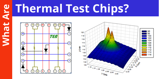
Thermal Test Chips
Thermal Test Chips

To meet aggressive product time-to-market goals, electrical and mechanical engineers need to work concurrently to envision, model and validate an enormous array of interdependent system requirements. While there’s no doubt that robust thermal modeling of both the semiconductor chip and heat sink solution help get ahead of the development curve, there is no substitute for actual test data. But, how do you do that before the final semiconductor chip, along with the associated product costs, is available. Enter the thermal test chip. They can be a convenient, fast and cost effective approach for developing package and cooling solutions at the individual semiconductor and system levels.
What Are Thermal Test Chips?
Thermal test chips are designed to help thermal engineers answer critical thermal packaging or material questions and can be divided into two groups.
- Application Specific Test Chips – Designed to mimic complex heat generation topologies such as those found in multi-core processors, system-on-a-chip, and power management and control designs, these thermal test chips are made to match a specific design. They are usually designed by the manufacturer of the corresponding application chip as a tool to help their customers get started on thermal design efforts well before the application chip design and fabrication is done.
- General Purpose Test Chips – Like their application specific counterpart, general purpose chips allow engineers to model, measure, and modify silicon design early in the processes. These chips have a standardized design in order to accommodate a wide variety of applications quickly and cost effectively. Yet, customization of the thermal profile and package is still possible.
Let’s take a slightly more in depth look at how one northern California company, Thermal Engineering Associates (TEA), implements these general purpose products.
Goals of General Purpose Thermal Test Chips (TTC)
To be useful to chip designers, TTCs need to meet several requirements including:
- Chip size that closely approximates the chip being simulated.
- Maximum possible heating area relative to chip size (JDEC standards specify a minimum of 85%)
- Uniform temperature profile across the heating area with the ability to simulate hotspots in specific areas.
- The ability to manipulate and measure different temperature profiles using standard lab equipment.
Design Implementation
TEA uses a ‘Unit Cell’ approach for its general purpose test chips that are manufactured in either flip chip or wire bond versions. Each unit cell is small (1mm or 2.54mm squared) yet can be arrayed into larger shapes up to 20 x 20 unit cells in order to mimic the final application specific chip. As shown below, each unit cell uses metal film resistors for heat flux generation and PN Junction diode(s) for temperature sensing. Power densities of ~300 W/cm2 and ~200 W/cm2 can be achieved for 1mm and 2.54mm unit cells respectively.
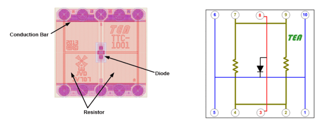
1mm X 1mm Unit Cell (TTC-1001)
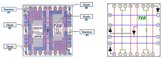
2.54mm X 2.54mm Unit Cell (TTC-14002)
Each 2.5mm unit cell has two resistors for heat generation and four diodes for temperature sensing while the 1mm unit cell includes two resistors and one temperature sensor. When configured and tested in an array using a given heat sink, it’s easy to see the precision and versatility of these general purpose test chips.
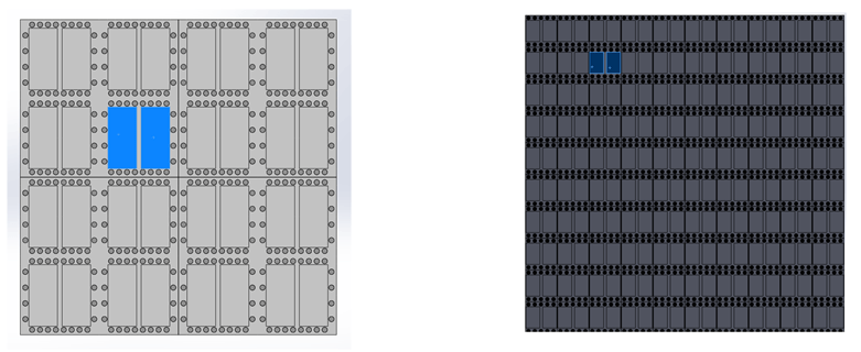
(L) 2.54mm Unit Cell in 4×4 Array (R) 1mm Unit Cell in 10×10 Array
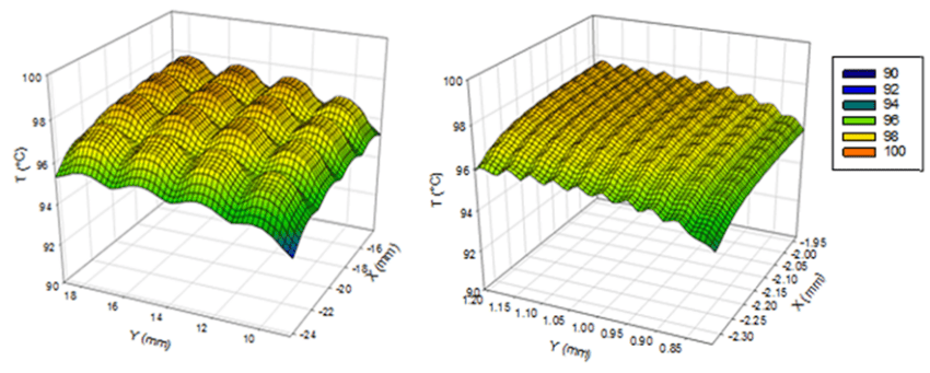
Uniform Temperature Distribution (L) 4×4 Array (R) 10×10 Array
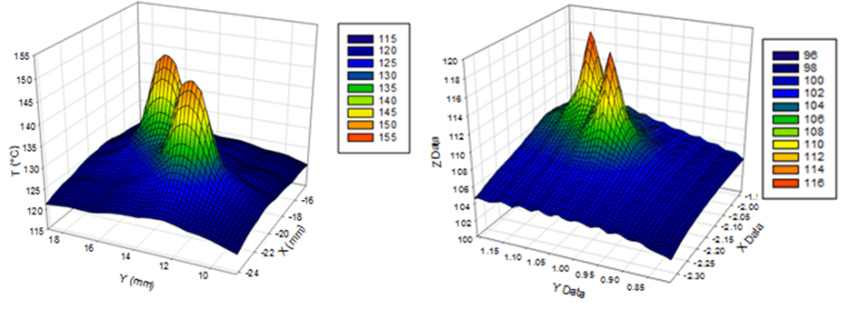
Two Hot Spots (L) 4×4 Array (R) 10×10 Array
The use of specialized thermal test chips is a convenient and efficient approach for developing package and cooling solutions. Thermal test chips, as compared to live device measurements, provide measurement accuracy and the ability to simulate high power density areas. Measurement data acquisition is simplified allowing the use of standard lab equipment for powering the resistors and sensing temperatures. No specialized switching equipment is required, reducing the cost for thermal test. The thermal test chip is also suited for advanced development of stacked, 2.5 and 3D packaging and in some cases is the only way temperatures can be detected in a stacked or 3D configuration.
Special thanks to Bernie Siegal of TEA and Tom Tartar of Package Science Services for providing us with information about general purpose thermal test chips. For more information, please visit the TEA website.
Related Links